Glossary of Memory and Memory Terms
Access time
1. The average time interval between a storage peripheral (usually a disk drive or semiconductor memory) receiving a request to read or write a certain location and returning the value read or completing the write.
2. A measurement of time in nanoseconds (ns) used to indicate the speed of memory. Access time is a cycle that begins the moment the CPU sends a request to memory and ends the moment the CPU receives the data it requested. Memory modules complete this process in as fast as 6ns for PC-133 MHz memory, while older modules can take up to 80ns or more.
Ambyx test system
Also called 'Ambyx Oven.' A burn-in and test system, developed by Micron, that performs burn-in and many functional tests under high-stress conditions to ensure long-term quality and reliability of our parts.
Amray
A machine that measures critical dimensions of designated areas on the die at different process levels through the use of a SEM (Scanning Electron Microscope).
Application specific processor
Highly integrated logic chip designed for specific applications to work alongside a microprocessor (e.g., a math co-processor, graphics processor, artificial intelligence processor, LAN processor, digital signal processor). These chips offload some of the specialized number crunching from the MPU.
Array
The area of the RAM that stores the bits. The array consists of rows and columns, with a cell at each intersection that can store a bit. The large rectangular section in the center of the die where the memory is stored.
ASCII
(American Standard Code for Information Interchange) A method of encoding text as binary values. The ASCII system requires nearly 256 combinations of 8-bit binary numbers to support every possible keystroke from the keyboard.
Asynchronous
A process in a multitasking system whose execution can proceed independently, "in the background.
Asynchronous Cache
Describes a type of L2 cache that is not in synch with the system clock. Asynchronous cache is slower than its synchronous counterpart, but is capable of delivering information to the CPU at a rate 10 percent faster than standard DRAM. Asynchronous cache was first used to boost memory performance in 386 systems and is still widely used today.
Auto precharge
A Synchronous DRAM feature that allows the memory chip's circuitry to close a page automatically at the end of a burst.
Bandwidth
The capacity to move data on an electronic line such as a bus or a channel. In short, the amount of data moved relative to a specific time frame. It is expressed in bits, bytes, or Hertz (cycles) per second. Essentially, a measure of the capacity of data that can be moved between two points in a given period of time.
Bank
A slot or group of slots that must be populated with modules of like capacity and fulfill the data width requirement of the CPU.
Bank Schema
A method of diagramming memory configurations. The bank schema system consists of rows and columns that represent memory sockets on a system: rows indicate independent sockets and columns represent banks of sockets.
Bare board
A printed circuit board (PCB) that does not have any components on it.
BEDO
Burst EDO - A variant on EDO DRAM in which read or write cycles are batched in bursts of four. Burst EDO bus speeds will range from 40MHz to 66MHz, well above the 33MHz bus speeds that can be accomplished using Fast Page Mode or EDO DRAM.
BGA
Ball Grid Array - a square package with solder balls on the underside for mounting. Use of BGA allows die package size to be reduced by allowing more surface area for attachment. Smaller packaging allows more components to be mounted on a module making greater densities available. The smaller package improves heat dissipation improving performance. See CSP and FBGA.
Binary
A method of encoding numbers as a series of bits. The binary number system, also referred to as base 2, uses combinations of only two digits - 1 and 0.
BIOS
Basic Input Output System - often referred to as CMOS, the BIOS provides an interface for a computer's hardware and software. The BIOS configuration determines how your hardware is accessed.
Bit
Short for Binary Digit, the smallest unit of data that can be processed or stored by a computer. A bit can have a value of either 1 or 0. Bits make up 'computer' language the same way letters of an alphabet make up human languages. Different combinations of different bits form 'words' and 'sentences' (actually signals) that a computer understands. Before these words and sentences can be transmitted from the CPU to memory, or vice versa, they must be broken down into 8-bit segments called bytes. Older computers were designed to handle only 8-bit data segments, while newer models have progressed to 64-bit segments. This larger bit width capacity generally means better and faster computer performance.
Block
A physical unit of information in a logical record; block size is usually expressed in bytes.
Block diagram
A circuit or system drawing concerned with major functions and interconnections between functions.
Bond pad
Square metallic pads on the die where the ball bond is attached. The bond pad is used to find acceptable eye points.
Buffered memory
This is when there is so much memory the chipset needs assistance to deal with the large loading introduced by the large amounts of memory. A buffer isolates the memory from the controller to minimize the load the chipset sees. This means adding logic, particularly drivers, to a SIMM or DIMM to increase the output current. Buffering is used to overcome signal attenuation due to capacitive loading. Modules that are "buffered" usually have small buffer chips mounted on them.
Burn-in
The process of exercising an integrated circuit at elevated voltage and temperature. This process accelerates failure normally seen as "infant mortality" in a chip. (Those chips that would fail early during actual usage will fail during burn-in. Those that pass have a life expectancy much greater than that required for normal usage.)
Burst Mode
Bursting is a rapid data-transfer technique that automatically generates a block of data (a series of consecutive addresses) every time the processor requests a single address. The assumption is that the next data-address the processor will request will be sequential to the previous one. Bursting can be applied both to read operations (from memory) and write operations (to memory).
Bus
The central communication avenue in a PCs system board. It normally consists of a set of parallel wires or signal traces that connect the CPU, the memory, all input/output devices, and peripherals and allows data to be transferred from one system component to another. Busses come in a variety of bit widths and speeds. To prevent data bottlenecks, the components attached to a bus must operate at close to the same speed as the bus.
Bus cycle
A single transaction occurring between the system memory and the CPU.
Byte
A unit of information made up of 8 bits. The byte is the fundamental unit of computer processing; almost all aspects of a computer's performance and specifications are measured in bytes or multiples of bytes such as kilobytes (~1,000 bytes) or megabytes (~1 million bytes), or gigabytes (~ 1 billion bytes)
Cache
A small fast area memory holding recently accessed data, designed to speed up subsequent access to the same data. Typically used between a processor and main memory.
Cache Controller
The circuit in control of the interface between the CPU, cache and DRAM (main memory).
Cache memory
Cache RAM is high-speed memory (usually SRAM) which is dedicated to storing frequently requested data. If the CPU needs data, it will check in the high-speed cache memory first before looking in the slower main memory. Cache memory may be three to five times faster than system DRAM. Most computers have two separate memory caches; L1 cache, located on the CPU, and L2 cache, located between the CPU and DRAM. L1 cache is faster than L2, and is the first place the CPU looks for its data. If data is not found in L1 cache, the search continues with the L2 cache, and then on to DRAM.
Capacitance
The property of a circuit element that allows it store an electrical charge.
Card Memory
A type of memory typically used in laptop and notebook computers. Credit card memory features a small for factor and is named for its similarity to the size of credit card.
CAS
(Column Address Select/or Strobe)--A control pin on a DRAM used to and activate a column address. The column selected on a DRAM is determined by the data present at the address pins when CAS becomes active.
CAS-RAS (CBR) (CAS before RAS)
CAS before RAS. Column Address Strobe Before Row Address Strobe. A fast refresh technique in which the DRAM keeps track of the next row it needs to refresh, thus simplifying what a system would have to do to refresh the part.
Catastrophic failure
When a device that was initially good now fails to function under any condition.
Check Bits
Extra data bits provided by a DRAM module to support ECC function. For a 4-byte bus, 7 or 8 check bits are needed to implement ECC, resulting in a total bus width of 39 or 40 bits. On an 8-byte bus, 8 additional bits are required, resulting in a bus width of 72 bits.
Checkboard
A detail test pattern designed to exercise each individual cell in the memory and find possible shorts between adjacent columns and data buses
CHMOS
Complementary High-density Metal Oxide Semiconductor.
CISC
Complex Instruction Set Computing. This design logic is usually associated with microprocessors. CISC chips use instructions, or commands, that involve several steps in one.
Clock Rate
The number of pulses emitted from a computer's clock in one second; it determines the rate at which logical or arithmetic gating is performed in a synchronous computer. An electrical current that alternates between high and low voltages. The speed of the clock is measured in Megahertz (MHz).
Clock Speed
The rate at which a computer's internal system clock operates. The clock is used to synchronize operations between the components within the clock.
CMOS
Complementary Metal Oxide Semiconductor. A process that uses both N- and P-channel devices in a complimentary fashion to achieve small geometries and low power consumption. On a PC CMOS generally refers to the BIOS information stored on a CMOS chip.
COAST
Cache On A Stick. Coast modules were used to upgrade a motherboard's L2 cache and Tag memory on some socket 7 and older motherboards.
COB
Chip On Board. A system in which semiconductor dice are mounted directly on a PC board and connected with bonded wires or solder bumps. The dice are usually mechanically protected with epoxy.
Column
Part of the memory array. A bit can be stored where a column and a row intersect.
Compact Flash Memory
A fast, postage stamp size RAM that is removable. The CF Card weighs half an ounce, with roughly one-fourth the volume and one-half the thickness of a PCMCIA Type II Card. The CF Card fits into a CF PC Card Adapter making it compatible with a standard PCMCIA Type II slot on any notebook or desktop computer. This allows the easy transfer of stored digital information from the CF Card to a computer or printer. Currently, the most readily available application for the CompactFlash Card is the digital still camera.
Controller
One of the major units in a computer that interprets and carries out the instructions in a program.
Coplanarity
With respect to semi-conductor packages, the condition of leads in a package having all elements, or all elements in a seating plane, between two parallel planes.
CPU
(Central Processing Unit)--The chip in a computer that has primary responsibility for interpreting commands and running programs. The CPU is the most vital component of a computer system. The speed of the CPU has a significant impact on overall system performance, but the CPU doesn't act alone. If slower memory is paired with a fast processor, the processor will be forced to wait for the memory to respond. When the speed mismatch is extreme, the user will see numerous memory errors and even complete system failure.
CRIMM
Continuity RIMMs are used to fill all unused RIMM sockets in a system. CRIMMs do not use any active components, and are used to continue the channel so that the signal can be properly terminated at the motherboard.
CSP
Chip Scale Package. CSP is a type of BGA in which the package is roughly the size of the die. CSP is also known as mBGA or micro-BGA.
Damping
In resonant circuits, the decay of oscillations due to the resistance in the circuit.
Data out
The signal line that carries the data read from the RAM (Random Access Memory).
Date code
A marking on all PCB and DRAM components indicating the manufacturing date of the product.
DDR
(Double Data Rate) or SDRAM II--The next generation of the current SDRAM. DDR finds its foundations on the same design core of SDRAM, yet adds advances to enhance its speed capabilities. As a result, DDR allows data to be sent on both the rising and falling edges of clock cycles in a data burst, delivering twice the bandwidth of standard SDRAMS. DDR essentially doubles the memory speed from SDRAMs without increasing the clock frequency.
Die
An individual rectangular pattern on a wafer that contains circuitry to perform a specific function. The internal circuitry is made of thousands of tiny electronic parts. 'Die' refers to a semiconductor component or part that has not yet been packaged (also known as 'IC' (Integrated Circuit) or 'chip').
Die pick-up tool
The bondhead tool on the machine that picks up the die from the precisor and places it on the leadframe.
Die size
The physical measurements of the die.
Dielectric
A material that conducts no current when it has voltage applied to it. Two dielectrics used in semiconductor processing are silicon dioxide and silicon nitride.
Dielectric deposition
A layer of deposited oxide used to isolate metal 1 from metal 2 on double-level metal processes. This must be done in such a way to prevent hillock formation on level 1.
Diffusion
The intermingling of molecules of two or more substances. When high temperature processes are done in diffusion tubes, the high temperature accelerates diffusion. Typical diffusion furnace temperature is 950 degrees Centigrade, or 1742 degrees Fahrenheit.
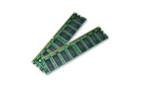
DIMM
Dual Inline Memory Module. A printed circuit board with gold or tin/lead contacts and memory devices. A DIMM is similar to a SIMM, but with this primary difference: unlike the leads on either side of a SIMM, which are "tied together" electrically, the leads on either side of a DIMM are electrically independent, ie actually separate circuits which allows for wider and faster data transfer.
DIP
(Dual In-line Package) A form of DRAM component packaging. DIPs can be installed either in sockets or permanently soldered into holes extending into the surface of the printed circuit board. The DIP package was extremely popular when it was common for memory to be installed directly on a computer's motherboard.
DQM
Data mask signal used by SDRAMs to provide byte masking during write operations. There is one DQM signal for every 8 bits of data width.
Direct address
A computer memory address that is included as part of the instruction.
Direct memory access
A computer feature that allows peripheral systems to access the memory for both read and write operations without affecting the state of the computer's central processor.
Distributed processing
Systems using intelligent input/output controllers and direct - memory - access control to free the CPU of the details of block transfers.
Doping
The introduction of an element that alters the conductivity of a semiconductor. Adding boron to silicon will create a P-type (more positive) material, while adding phosphorus or arsenic to silicon will create N-type (more negative) material.
DRAM
(Dynamic Random Access Memory) DRAM is the most common type of memory and is "dynamic" because in order for the memory chip to retain data, it must be refreshed constantly ( a pulse of current through all of the memory cells every few milliseconds). If the cell is not refreshed, the data is lost. DRAM temporarily stores data in a cell composed of a capacitor and a transistor. Each cell contains a specified number of bits. These cells are accessed by row addresses and column addresses. (See also RAM and SRAM.)
DRDRAM
(Direct Rambus DRAM) A totally new RAM architecture, complete with bus mastering (the Rambus Channel Master) and a new pathway (the Rambus Channel) between memory devices (the Rambus Channel Slaves). A single Rambus Channel has the potential to reach 500MBp/s to 800Mb/s in burst mode; a 20-fold increase over DRAM.
Driver board
A printed circuit board that sends signals from the interface board of the oven to the DUT board and back to the interface board. Each oven slot has a corresponding driver board located in the back of the oven.
Dry pack
The process of preparing product for shipment in moisture vapor barrier bags. This process includes tubed or reeled product and a clay desiccant, and an HIC (Humidity Indicator Card), vacuum-sealed in a moisture vapor barrier bag.
DUT
Device Under Test. It is used interchangeably with UUT (Unit Under Test).
Dynamic
Type of RAM (Random Access Memory). To keep data in the D(ynamic)RAM memory, this data needs to be 'refreshed' (recharged). The electric charge fades out of a DRAM like air seeps out of a balloon. Because of this change, it is called Dynamic.
E2PROM
Electrically Erasable PROM.
EAROM
Electrically Alterable Read-Only Memory.
ECC
Error Correction Code. A method used to check the integrity of data stored in memory . ECC memory improves data integrity by detecting errors in memory and is more advanced than parity because it can detect both multiple-bit errors and single-bit errors (parity only detects single-bit errors). ECC is typically found in high-end PCs and file servers where data integrity is key. An ECC scheme capability is partially determined by the sophistication of the "systematic code" employed. The systematic code is like a reference table that the memory system uses to determine whether or not the memory has returned the correct data. Every time data is stored in memory, this code is responsible for the generation of check bits which are stored along with the data. When the contents of a memory location is referenced, the ECC memory logic uses the check bit information and the data itself to generate a series of "syndrome bits". If these syndrome bits are all zeros, then the data is valid and operation continues. If any bits are ones, then the data has an error and the ECC memory logic isolates the errors and reports them in the operating system. In the case of a correctable error, the ECC memory scheme can detect single and double bit errors and correct single bit errors.
EDO
A memory feature that allows for faster back to back accesses.
EDO Parity RAM
EDO Parity RAM offers the high performance of EDO memory and has built-in parity which greatly improves reliability. Ideal for high-end PCs and entry-level servers, EDO Parity modules are compatible with any system that accepts a standard 72-pin EDO module and are rapidly becoming the new standard on high-end systems.
EDO RAM
(Extended Data Out) EDO RAM is similar to FPM memory, a form of DRAM technology that shortens the read cycle between memory and CPU. but provides improved performance by keeping available data longer in memory. It eliminates much of the wait time by allowing the processor to access data during the refresh cycle. In other words, the computer can load data as it is searching for new information. EDO memory is generally 10 to 20% faster than FPM memory. A computer must support EDO memory in order to notice an increase in performance.
EDRAM
(Enhanced Dynamic Random Access Memory)--a form of DRAM that boosts performance by placing a small complement of static RAM (SRAM) in each DRAM chip and using the SRAM as a cache. Also known as cached DRAM, or CDRAM.
EEPLD
Electrically Erasable Programmable Logic Device. A CMOS PLD made by using EEPROM technology. It can be erased and reprogrammed.
EEPROM
Electrically Erasable, Programmable, Read-Only Memory chip. EEPROMs differ from DRAMs in that the memory stays in even if electrical power is lost. Also, the memory can be erased and reprogrammed.
Electrostatic discharge (ESD)
The dissipation of electricity. ESD can easily destroy semiconductor products.
EOB
End Of Buffer.
EPROM
Electrically Erasable, PROgrammable, Read-Only Memory chip. EEPROMs differ from DRAMs in that the memory stays in even if electrical power is lost. Also, the memory can be erased and reprogrammed.
EOS
(ECC on SIMM) A data-integrity checking technology designed by IBM that features ECC data-integrity checking built onto a SIMM.
EPROM
Erasable Programmable Read Only Memory
Encapsulation
The process of applying a cured-plastic protective housing to components. A mold compound. An Assembly step.
Etch
A process using a chemical bath (wet etch) or a plasma (dry etch) that removes unwanted substances from the wafer surface.
Ethernet
A local area network allowing several computers to transfer data on a communications cable.
Even Parity
Even parity and odd parity are two different parity protocols used to check the integrity of data stored in memory. A memory manufacturer can use either protocol in a memory product. Even parity adds an additional bit to every byte of data to make the total number of 1's in the segment even. When the byte passes to the CPU, the parity circuit checks the byte to be sure it is still even. If it is, the data is considered to be valid and the parity bit is removed from the byte. If instead it registers as odd, it is considered to be invalid and a parity error is generated.
Failure rate
Description of the rate at which parts fail, usually expressed as percent per 1,000,000.
Fake Parity
Unlike odd and even parity, fake parity is not capable of detecting an invalid data bit. It was designed to artificially 'satisfy' a parity-enabled computer without actually checking the data for errors. Fake parity attaches a bit to each byte of data just like odd and even parity protocols. The difference is that fake parity simply adds the correct parity bit as the data is sent to the CPU instead of attaching it before the data is stored to memory, and recalculating it before the byte passes to the CPU.
Fall out
Material that fails various tests within the component manufacturing process.
FBGA
Fine BGA is a ball grid array package with a fine pitch ball arrangement on the underside of the package (larger than CSP).
FIT
Failures In Time.
FSB
Front Side Bus is the data channel connecting the processor, chipset, DRAM, and AGP socket. FSB is described in terms of its width in bits and it's speed in MHz.
Flag
In computing: A status bit that causes some indication of the state or condition of the processing unit.
Flash memory
Flash memory is a non-volatile memory device that retains its data when the power is removed. The device is similar to EPROM with the exception that it can be electrically erased, whereas an EPROM must be exposed to ultra-violet light to erase. Flash memory does not need a constant power supply to retain its data and it offers extremely fast access times, low power consumption, and relative immunity to severe shock or vibration. These qualities combined with its compact size, make it perfect for portable devices like scanners digital cameras, cell phones, pagers, hand-helds and printers. Flash chips have a lifespan limited to 100,000 write cycles, which means flash will never replace main memory in computers.
Flatpack(1)
A Teflon Polyurethane wafer holder used to transport individual wafers. Flatpacks can be stacked to carry and protect several wafers at a time.
Flatpack(2)
A flat, rectangular IC package type with leads sticking out from the sides of the package.
Flip-flop
A circuit with two stable states that can be changed from one to the other. Flip-flops are the storage element in most of the SRAMs.
Floating
Pertaining to the condition of a device or circuit that is neither grounded nor connected to any potential. (Potential is voltage course or current course).
Floating gate
In Silicon Gate MOS technology: a gate that is not directly connected to the rest of the circuit. Used in EEPROMs.
FPM
Fast Page Mode - A common DRAM data-access scheme. Accessing DRAM is similar to finding information in a book. First, you turn to a particular page, then you select information from the page. Fast-page mode enables the CPU to access new data in half the normal access time, as long as it is on the same page as the previous request. This feature is used to support faster sequential access to DRAM by allowing any number of accesses to the currently open row to be made after supplying the row address just once.
Frequency converter
A device or system that can change the frequency of an alternating current, whether or not it changes the voltage or phase.
Gigabit
Approximately 1 billion bits: 1 bit x 1,024 (that is, 1,073,741,824 bits) Or exactly 2^30 bits.
Gigabyte, GB
A unit of measurement approximately equal to 1024 megabytes. Computer components process data in bytes or multiples of bytes such as kilobytes (~1,000 bytes), megabytes (~1 million bytes), and gigabytes (~ 1 billion bytes).
GND
Ground.
Gold wire
The wire used to make a physical connection from the device to the leadframe.
Hard failure
Die that fail functionality testing. These failures have a visual defect 99 percent time, such as poly or metal bridging, missing geometries or layers, particles or contaminates.
Heat sink
A structure, attached to or part of a semiconductor device that serves the purpose of dissipating heat to the surrounding environment; usually metallic. Some packages serve as heat sinks.
HPM
Hyper Page Mode also known as EDO.
HTOL
High Temperature Operating Life.
I/O port
Connection to a CPU that is configured or programmed to provide data path between the CPU and external devices such as a keyboard, display, or reader; it may be an input port or an output port, or it may be bi-directional.
IC
Integrated Circuit. A tiny complex of electronic components and their connections that is produced in or on a small slice of material (as silicon).
ICE
In Circuit Emulator.
ID
Identification Detect. Pins present on DIMMs to provide information to the system using the module.
IEEE-488
Standard set by IEEE (Institute of Electrical and Electronics Engineers) for communication between pieces of electronic apparatus.
Infant Mortality
Used to describe the occurrence of premature failures at a higher than normal rate.
Intelligent
A burn-in process whereby electrical functionality of the parts is continuously or periodically monitored and recorded under various voltages, temperatures, and refresh conditions during the burn-in process. This continuous or periodic monitoring of the functionality of each IC allows intelligent decisions to be made.
IO CARD
A PCB that interfaces between the computer and an interface board.
IR
Current x Resistance = Voltage. Also an abbreviation for Infrared.
ISD
An amorphous, doped polysilicon used as an underlying layer for the HSG poly to increase conductivity.
ISO 9
International Standards Organization.
JEDEC
Joint Electron Device Engineering Council - the group that establishes the industry standards for memory operation, features and packaging.
Back To Top To Top
Keys
Notches on a memory module that prevent it from being installed incorrectly or into an incompatible system.
Kilobit Approximately one thousand bits: 1 bit x 210 (that is, 1,024 bits).
Kilobyte, KB
A unit of measurement approximately equal to 1024 bytes. Computer components process data in bytes or multiples of bytes such as kilobytes (~1,000 bytes), megabytes (~1 million bytes), and gigabytes (~ 1 billion bytes).
L1 cache
Level 1 cache. A small cache integrated in processor that provides a small working space for quick access to the most recently used data.
L2 cache
A specialized memory unit that enhances DRAM performance by providing the CPU with data at speeds ten times faster than DRAM. The L2 cache is comprised of Static RAM (SRAM), a high-speed RAM that does not need to be refreshed to retain its data. Most computers have two different memory caches; L1 cache, located on the CPU, and L2 cache, located between the CPU and DRAM. L1 cache is faster than L2, and is the first place the CPU looks for its data. If data is not found in L1 cache, the search continues to the L2 cache and then to DRAM. In early processors, the L2 cache was not integrated into the processor but rather built into the motherboard, and was in some cases upgradeable. See COAST.
Laser scribe
Process which uses a YAG (Yittrium-aluminum-Garnet) laser to melt the silicon in a dot matrix to form wafer scribe numbers.
Latch
Circuit element that stores a given value on its output until told to store a different value.
Latch up
An undesired phenomenon in an integrated circuit whereby a circuit locks in a certain state and will not change.
Latch voltage
The effective input voltage at which a flip-flop changes states.
Lead
The metal extensions from an IC package or discrete component that connects the component to the PCB. The leg or contact point of the component that is either physically soldered to a PC board or placed within a socket for connection.
Leadframe
A metal structure that is part of the device. The die is attached to the leadframe.
Leads
Leads or Legs: The official name for the metal 'feet' on an IC. Also called 'pins.' The part of the lead assembly that is formed after a portion of the lead frame is cut away. The part's connection to the outside world.
Leakage
Undesirable conductive paths in components, subsystems, and systems; also the current through such paths.
Life testing
Accelerated testing of electronic components to establish their field reliability.
Linear circuit
A circuit that produces a voltage output approximately proportional to the input voltage, generally over a limited range of voltage frequency.
Linear regulator
Power supply design in which the voltage is held constant by dissipating 50% of the input voltage times and output current as a margin.
Linear selection
A method of selecting memory or input/output devices that dedicates one address line per chip selection; results in overlapping or noncontiguous memory; used because it is the cheapest method of selection.
Locator pin
A pin in the mold which locates the leadframe in the correct position on the mold for processing.
Logic Board
(See motherboard)
Logic circuit
An integrated circuit which provides a fixed set of output signals according to the signals present at the input.
Logic gate
Several individual device functions on an integrated circuit chip.
Marching
Detail test pattern designed to check for decoder and cell interaction problems.
Megabit
Amount of memory equal to 1 bit x 1,0242 or 1,048,576 bits of information. (Abbreviated Mb.)
Megabyte
Amount of memory equal to 1,048,576 bytes of information. (Abbreviated MB.)
Memory
A Term commonly used to refer to computer system's random access memory (see also RAM). The term memory has also been used to refer to all types of electronic data storage (see storage). A computer system's memory is crucial to its operation; without memory, a computer could not read programs or retain data. Memory stores data electronically in memory cells contained in chips. The two most common types of memory chips are DRAM and SRAM.
Memory Bank
A logical unit of memory in a computer, the size of which is determined by the computer's CPU. For example, a 32-bit CPU calls for memory banks that provide 32 bits of information at a time.
Memory Configuration
The amount of memory in an IC and how it is accessed. Also, a code on the lot traveler used to indicate the IC's memory configuration (e.g., 1M1 = 1 Meg x 1, 4M4 = 4 Meg x 4, etc.).
Memory Controller
The logic chip used to handle the I/O (input/output) of data going to and from memory. See chipset.
Memory Cycle
Minimum amount of time required for a memory to complete a cycle such as read, write, read/write, or read/modify/write.
Memory Types:
- Cache Data SRAM: quick-access chip.
- DRAM dynamic random access memory.
- SDRAM synchronous dynamic random access memory.
- DDR SDRAM double data rate dynamic random access memory.
- SLDRAM synchronous link dynamic random access memory.
- RDRAM (also DRDRAM) Rambus dynamic random access memory.
- EPROM: erasable, programmable, read-only memory.
- PROM: programmable, read-only memory.
- RAM: random access memory.
- ROM: read-only memory (permanent memory that cannot be changed).
- SRAM: static random access memory.
MHz
Megahertz is a measurement of clock cycles in millions of cycles per second.
Micron
A unit of measure equivalent to one-millionth of a meter; synonymous with micrometer.
MIPS
Millions of Instructions Per Second. This measurement is generally used when describing the speed of computer systems.
MNOS
Metal Nitride Oxide Semiconductor. The technology used for EAROMs (Electrically Alterable ROMs); not to be confused with NMOS.
Moisture vapor barrier bag
A vacuum-sealed bag designed to keep the moisture out so that the parts inside will not be damaged.
Monolithic
Contained on one chip or substrate, as a microprocessor system including not only the logic but also memory or input/output circuits.
MOS
Metal-Oxide-Semiconductor. Layers used to create a semiconductor circuit. A thin insulating layer of oxide is deposited on the surface of the wafer. Then a highly conductive layer of tungsten silicide is placed over the top of the oxide dielectric.
MOS device
Device in which current flow occurs in a single channel of P- or N-type material and is controlled by an insulated electrode on the surface of the channel region.
MOS process
The set of chemical and metallurgical steps used to make MOS Large Scale Integration.
MOST
Metal Oxide Semiconductor Transistor.
Motherboard (also known as Mainboard)
Also known as logic board, main board, or system board; your computer's main electronics board, which in most cases either contains all CPU, memory, and I/0 functions, or has expansion slots that support them.
MTBF
Mean Time Between Failures.
MTTF
Mean Time To Failure.
MU
Memory Unit. Usually a printed circuit board assembly populated with memory chips that stores a certain quantity of memory. Intel term for one of the types of cards in a memory system card set.
Nand
A computer logic circuit that produces an output which is the inverse of that of an AND circuit.
Nano
Literal: One-billionth (10 to the -9). Diffusion: A tool used to measure the thickness of a film on a wafer.
Nanometer
One billionth of a meter.
Nanosecond (ns)
One billionth of a second. Memory data access times are measured in nanoseconds. For example, memory access times for typical 30- and 72-pin SIMM modules range from 60 to 100 nanoseconds.
NC
Not Connected.
Negative charge
Charge caused by the presence of electrons, not their absence.
Newton
A unit of force in the meter-kilogram-second system needed to accelerate a mass of one kilogram one meter per second per second.
Nibble
Usually 4 bits or half a byte.
NMOS
N-channel Metal Oxide Semiconductor. This pertains to MOS devices constructed on a P-type substrate in which electrons flow between N-type source and drain contacts. NMOS devices are typically two to three times faster than PMOS devices.
Noncomposite
A term created by Apple Computer, Inc. that describes a memory module which uses 16-Mbit technology. For a given capacity, a noncomposite module will have fewer chips than a composite module.
Nonvolatile memory
Types of memory that retain their contents when power is turned off. ROMs, PROMs, EPROMs and flash memory are examples. Sometimes the term refers to memory that is inherently volatile, but maintains its content because it is connected to a battery at all times, such as CMOS memory and to storage systems, such as hard disks.
NOR
Logical NOT-OR.
NS (ns)
Nanosecond (ns). One billionth of a second; used to measure the speed of the parts (e.g., -07 nanoseconds).
NVRAM
Non-Volatile Random Access Memory.
Odd Parity
Even parity and odd parity are two different parity protocols used to check the integrity of data stored in memory. A memory manufacturer can use either protocol in a memory product. Odd parity adds an additional bit to every byte of data to make the total number of 1s odd. When the byte passes to the CPU, the parity circuit checks the byte to be sure it is still odd. If it is, the data is considered to be valid and the parity bit is stripped from the byte. If instead it registers as even, it is considered to be invalid and a parity error is generated.
OE
Output-Enable. On a part, where data-in and data-out are shared on the same pins, the OE must be triggered to request output data.
OHM
A unit of measure of electrical resistance.
Open
A circuit interruption that results in an incomplete path for the current flow. (e.g., an open wire which opens the path of the current).
Operating system
Software controlling the overall operation of a multipurpose computer system, including such tasks as memory allocation, input and output distribution, interrupt processing, and job scheduling.
Operational amplifier
An electronic circuit which amplifies 'linear' (also called analog) signals.
Pad
A conductive bonding island located strategically on circuit chips for inter-connecting circuit elements or for bringing connections from circuit leads to the outside.
Page
The number of bits that can be accessed from one row address.
Page mode
Mode in which if RAS is kept low and the DRAM is given a column-address without being given a new row-address, the chip will remember which row it was on the last time and automatically stay on that row. It is like saying that all the bits along one row are all on the same 'page,' and the part will assume the same page is intended until a different page is specified.
PAL
Programmable Array Logic. A device that can be programmed to do certain logic functions. Then a fuse inside of the device can be blown so the programmed information can never be changed. Sometimes called a PLD (Programmable Logic Device) Language.
Parametric fail
A test of the DUT that checks for pin leakage, the amount of current it draws, opens, and shorts.
Parametric test
A test that measures values, also called a dynamic test as opposed to a functional or Go/No-Go test.
Parametrics
A series of voltage and current tests performed on all products in Probe. The test checks for variations in the fabrication process. Test results are used by engineers to modify or correct processes.
Parity
A quality control method that checks the integrity of data stored in a computer's memory. Parity works by adding an extra bit of data to each byte to make the total number of 1's either odd or even An error is detected if the parity circuit determines that this number has changed, indicating that some of the data may have been lost or otherwise corrupted. Two different parity protocols exist, even parity and odd parity. Parity protocols are capable of detecting single bit errors only. To enable multiple-bit error detection, manufacturers must use a more advanced form of error checking called Error Correcting Code (ECC). See also Fake Parity.
Parity Bit
A bit added to a group of bits to detect the presence of an error.
Parser
The portion of a language translator (compiler or assembler) which determines the logical structure of the program being completed.
Passive device
A device incapable of current gain or switching such as a resistor or capacitor.
Passive element
A circuit element without an energy source such as a capacitor or resistor.
PC100
Intel's PC100 specification defines the requirements for SDRAM used on 100 MHz FSB motherboards. Around the middle of 1998, Intel introduced the BX chip set to their motherboard designs. One element in this new architecture will include an increase in the PC main memory bus speed (Host bus) from 66 to 100 MHz, called PC 100. To match the 100MHz bus speed, 100MHz SDRAM modules is the required memory technology for this new chip set.
PC133
The PC133 specification details the requirements for SDRAM used on 133MHz FSB motherboards. PC133 SDRAM can be used on 100MHz FSB motherboards but will not yield a performance advantage over PC100 memory at 100MHz.
PCB
(Printed Circuit Board) A component made up of layers of copper and fiberglass; the surface of a PCB features a pattern of copper lines, or "traces," that provide electrical connections for chips and other components that mount on the surface of the PCB. Examples: motherboard, SIMM, credit card memory, and so on.
PCMCIA
(Personal Computer Memory Card International Association) A standard that allows interchangeability of various computing components on the same connector. The PCMCIA standard is designed to support input/ output devices, including memory, fax/modem, SCSI, and networking products.
PD
Presence Detect. Indicator pins on SIMMs and DIMMs that provide information to the system using the module.
PGA
Pin Grid Array.
Pin
The metal extensions from an IC package or discrete component that connects the component to the PCB.
Pin one hole
The hole located on the 'pin one' side of the leadframe.
Pin-one indicator
An indentation or mark on the top of the part that indicates where the first lead of the die inside is located.
Pipeline Burst Cache
A type of synchronous cache that uses two techniques to minimise processor wait states - a burst mode that pre-fetches memory contents before they are requested, and pipelining so that one memory value can be accessed in the cache at the same time that another memory value is accessed in DRAM.
PLA
Programmable Logic Array. An array of logic elements that can be programmed to perform a specific logic function. It can be as simple as a gate or as complex as a ROM and can be programmed (often by mask programming) so that a given input combination produces a known output function.
PLD
Programmable Logic Devices. Devices with 10-100 times higher level of integration than a TTL; called programmable because they can be customized in software rather than in hardware.
PMOS
P-channel Metal Oxide Semiconductor. This pertains to MOS devices constructed on an N-type silicon substrate in which holes flow between source and drain contacts.
Polyimide
Protective covering over the die; also called Die Coat
Polysilicon
Poly-crystalline layer of silicon used for the silicon gate contact in silicon gate MOS devices; also used for interconnections between devices.
Populated board
A PCB with components.
Power down
To turn the system's power OFF.
Power up
To turn the system's power ON.
PQFP
Plastic Quad Flat Pack. A square, flat package with gullwing leads located around all four sides of the package.
Primary Cache
Cache that is closest to the processor: typically located inside the CPU chip. Can be implemented either as a unified cache or as separate sections for instructions and data. Also referred to as Level 1 cache or internal cache.
Probe
Wire used to make electrical contact with a pad on a die; usually made of either beryllium copper, tungsten, or palladium. The diameter of the probe shank is 10 mils, the diameter of the standard probe tip is 1.5 mils, and the length is 7 or 14 mils.
Probe card
A fiberglass card (P.C. Board) that has a hole in the center in which there are pins that are aligned and placed on pads located on the die. As the pins on the probe card are placed on die pads, the probe card tests and sorts die for functionality.
Proprietary Memory
Memory that is custom-designed for a specific computer.
Pull-up
A device or method used to keep the output voltage of a device at a high level; often a resistor network connected to a positive supply voltage.
PWB
Printed Wiring Board; board upon which there are layers of printed circuits where DRAMs can be attached with solder so that memory can be accessed.
Quad flat pack
QFP: A flat, rectangular, integrated circuit with its leads projecting from all four sides of the package without radius.
RAM
Random Access Memory - A type of memory that can be written to and read from in a nonlinear (random) manner. When an application is opened. it is transferred from the hard drive to RAM where it is more readily accessible. RAM enhances system performance because it can process requests from the CPU more quickly than the hard drive. The kind of RAM used in main memory on most computers is Dynamic RAM (DRAM). DRAM stores data as electronic signals. These signals must be constantly refreshed to keep them from dissipating. The more RAM your computer has, the more data it can store at one time and subsequently the more efficiently your computer will operate. The data held in RAM is lost when the computer is turned off. The term random derives from the fact that the CPU can retrieve data from any individual location, or address, within RAM.
Ramp
A period of time in the oven when the temperature goes up.
Random failure region
The portion of the bathtub curve that represents the useful portion of device life.
Range
The difference between the smallest and largest values in a set of data. This is the simplest measure of variation.
RAS
Row-Address-Strobe: the signal that tells the DRAM to accept the given address as a row-address. Used with CAS and a column-address to select a bit within the DRAM.
RDRAM
Rambus DRAM is an evolutionary type of DRAM that uses a 16-18 bit data path and is designed to operate with FSB speed of 800 MHz producing a burst transfer rate of 1.6 gigahertz. Rambus DRAM technology is a system-wide, chip-to-chip interface design that allows data to pass through a simplified bus. Rambus uses a unique RSL (Rambus Signaling Logic) technology. Rambus is available in two flavors: RDRAM and Concurrent RDRAM. The third line extension, Direct RDRAM, was developed in stages and went into production in 1999. In late 1996, Rambus agreed to a development and license contract with Intel that lead to Intel's i820 and i840 chip sets supporting Rambus memory being released in 1999.
Read time
The amount of time required for the output data to become valid once the read and address inputs have been enabled; generally called access time.
Read-restore
A mode of operation used in core memory systems.
Read/write memory
A generic term for Random Access Memories.
Refresh
An electrical process used to maintain data stored in DRAM. The process of refreshing electrical cells on a DRAM component is similar to that of recharging batteries. Different DRAM components call for different refresh methods.
Refresh rate
This is a count of the number of rows (in thousands) refreshed at a time in a refresh cycle. Common refresh rates are 1K, 2K, and 4K. DRAM stores data as a series of electron charges in individual cells. This data must be constantly recharged or 'refreshed' to keep the data from dissipating. The refresh rate refers to the size of the data that must be recharged, and is typically expressed in kilobytes (~1,000 bytes). Two common refresh rates are 2K and 4K, with 2K being the faster rate.
Registered memory
Registers delay memory information for one clock cycle to ensure all communication from the chipset is collected by the clock edge, providing a controlled delay on heavily loaded memories.
Relative address
An identifier that indicates the position of a memory location in a computer routine relative to the base address as opposed to the memory location's absolute address.
Release time
The amount of time data must remain stable after a device or circuit has been clocked; also called 'hold time.'
Resist
A material that prevents etching or plating of the area it covers; also called photoresist.
RIMM
Rambus Inline Memory Modules used for RAMBUS DRAM. A form of chip packaging that is similar to DIMMs using Direct Rambus DRAM memory subsystems.
RISC
Reduced Instruction Set Computing. The design methodology is usually associated with microprocessors. RISC chips use simpler instructions, or commands, than CISC chips. However, they need to use more steps to perform many functions that CISC chips perform in one step. SPARC and MIPS chips are based on RISC.
Rise time
The amount of time required for a signal level change to increase from ten percent to ninety percent of its final specified value.
RMA
Returned Material Authorization; required if a customer desires to return products. Also refers to parts that have been returned from a customer.
ROM
Read Only Memory - A form of random access memory that can only be read from, not written to. Most systems use ROM to store the instructions a computer needs during the startup process.
Row
Part of the RAM array; a bit can be stored where a column and a row intersect.
Row/columns
Describes how many rows are on a wafer map in the X direction. (X = left to right. Y = top to bottom).
RPL
An acronym to represent RS/1 Programming Language. RPLs are functions or procedures written in RS/1's built in programming language. These RPLs are used to automate tasks and analyses.
RW
Read/Write memory.
Scribe
A marking on a wafer that identifies the wafer and the lot it came from. The scribe is located on the front of the wafer, opposite the major flat.
SDRAM
Synchronous Dynamic Random-Access Memory. A DRAM technology that uses a clock to synchronize signal input and output on a memory chip. The clock is coordinated with the CPU clock so the timing of the memory chips and the timing of the CPU are "in synch." The synchronization eliminates time delays and allows for fast consecutive read and write capability, thereby increasing the overall performance of the computer. SDRAM has two separate memory banks that operate simultaneously, while one bank prepares for access, the other is being accessed. SDRAM allows the CPU to access memory approximately 25 percent faster than EDO memory because it is controlled by the system clock. SDRAM can only be used in computers designed for it and cannot be mixed with any other type of memory. SDRAM can operate at 100MHz, 133Mhz and features a burst mode that allows it to address blocks of information instead of small data bits.
Secondary Cache
Cache that is second closest to the processor; typically located on the system board. Also referred to as Level 2 cache and external cache.
Self Refresh
A memory technology that enables DRAM to refresh on its own-independent of the CPU or external refresh circuitry. This technology is built into the DRAM chip itself and reduces power consumption dramatically. It is commonly used in notebook and laptop computers.
SER
Soft Error Rate. An error caused by temporary disruption of memory cell.
Serial Presence Detect (SPD)
Serial Presence Detect. An enhanced presence detect that uses an EEPROM to store modules timings, configuration, and the manufacturer's data.
Semiconductor
An element, such as silicon, that has intermediate in electrical conductivity between conductors and insulators, which conduction takes place by means of holes and electrons.
Sense amp
The sense amp acts as a distributor of current on the die.
Sense amplifier
A device or circuit capable of sensing very low voltages and amplifying them to some higher voltage level.
SGRAM
Syncronous Graphics RAM. A single port DRAM designed for graphics hardware that require high speed throughput such as 3-D rendering and full-motion video.
Shrink
A reduction in die (chip) size. A reduction in the size of the circuit design resulting in smaller die sizes that increases the number of possible die per wafer.
SIM
Single In-line Module. Same as SIP except with a connector edge instead of leads.
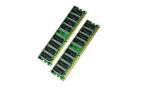
SIMM
Single In-line Memory Module - a high-density DRAM package alternative consisting of several components connected to a single printed circuit board. A small PCB designed to mount in a socket on a larger PCB providing a large memory upgrade in a small space. This board provides the connection between multiple memory chips and the computer system. SIMMS come in various pin configurations, the most common type being: 30 pin and 72 pin. A 30 pin SIMM has a row of 30 tin or gold pins long the bottom of the module which determine the amount of data the module can handle. These pins connect to only one memory chip as opposed to DIMMs which can connect to multiple chips.
SIMM socket
An interconnect component mounted on the system board, or motherboard, designed to hold a single SIMM.
SIP
Single In line Package. A component or module that has one row of leads along one side. Many resistors come in SIP form.
SLDRAM
Synchronous Link Dynamic Random Access Memory. SLDRAM is the next evolution of SDRAM using a multiplexed command bus allowing fewer pins to increase bandwidth and allow higher FSB speeds.
SODIMM
Small Outline Dual Inline Memory Module. Smaller and thinner than standard DIMMs, SODIMMs are typically used in laptop computers and mobile computing devices. An enhanced version of a standard DIMM. The small outline DIMM is about half the length of a typical 72-pin SIMM. SO DIMMs come in a variety of pin sizes and can be installed either singly to support 32-bit systems, or in pairs to support 64-bit systems.
Soft error
An error caused by a temporary disruption of the memory cell.
Soft error fail
A part with a temporary, single-bit failure during the soft error test.
SORIMM
Small Outline Rambus Inline Memory Module. SORIMMs have a smaller profile that standard RIMMs and are used in laptop computers and systems that have strict size requirements.
SOJ
Small Outline J-lead package. A rectangular package with leads sticking out of the side of the package. The leads are formed in a J-bend profile, bending underneath and towards the bottom of the package.
SPC
Statistical Process Control. The use of statistics to determine uniformity around a target value.
SPD (Serial Presence Detect)
An enhanced presence detect that uses an EEPROM to store manufacturer data.
Speed
The time it takes the RAM to put information into its memory or get information out of its memory. It is measured from the time that an address and proper control signals are given, until the information is stored or placed in the device's output(s).
Speed grade
Our coding for the speed that the stored information in the part can be retrieved by a computer. For DRAMs, a -5 is 50 nanoseconds, a -6 is 60 nanoseconds, a -7 is 70 nanoseconds, etc. For SRAMs, a -10 is 10 nanoseconds, etc.
SPHS
An operation found in coat and develop programs that stands for spin high speed.
Spike
The sudden drastic portion of a pulse that significantly exceeds its average amplitude. Standard deviation A measure of variation for a particular process or product characteristic. This is often abbreviated as 'STD DEV' or 'STD'.
SRA
Standard Readability Assessment.
SRAM
(Static Random Access Memory) An integrated circuit similar to a DRAM (Dynamic Random Access Memory) with the exception that the memory does not need to be refreshed. SRAM is faster and more expensive than DRAM and is generally used for speed-critical areas of the computer such as cache memory.
Starting address
Smallest or lowest address that a memory system will respond to.
Static ram
Unlike volatile memory, static memory retains its contents even when the main current is turned off. The trickle of electricity from a battery is enough to refresh it.
Storage Device
A medium designed to hold data, such as Floppy Diskette, Harrd Disk Drive or CD-ROM.
Strobe
An input that allows parallel data to be entered a synchronously.
Substrate
The actual structural material on which semiconductor devices are fabricated, whether passive or active. The term applies to any supportive material, such as the materials used in the fabrication of printed circuits.
Surface-mount package
A J-leaded or Gullwing package or BGA that can be mounted directly on the surface of P.C. Boards (as opposed to through-hole packages).
Switches menu
The menu in BIOS containing user-configurable options for a PC's hardware configuration.
Synchronous Cache
A kind of L2 cache that is synchronized with the CPU. This eliminates the lag time created while the CPU waits for cache memory to fulfill its requests. Synchronous cache is typically 3 to 5 percent faster than asynchronous cache, and is a full 20 percent faster than standard DRAM. See also Asynchronous Cache.
TAG
The subset of the CPU address bits used to compare the tag bits of the cache directory to the main memory address being accessed. Tag memory acts as an index for the information stored in L2 cache.
Tag RAM
Cache is physically divided into two sections. The Tag RAM section stores the Tag address of the location of the data in cache. This section is smaller than the Data RAM section, which stores the actual data or instruction.
TBD
To Be Determined. Used on quotes in reference to shipping dates.
TCAC
A measurement of the speed or how fast the part is; it is the time it takes to get a bit of information out of the part after CAS comes down.
TCE
Thermal Coefficient of Expansion. A constant that describes the changes in linear dimensions with respect to temperature for a device or material.
TG
A code for TSOP (see TSOP). A package-type code.
TSOP
Thin Small Outline Package. It is thinner and slightly smaller than an SOJ and with gullwing-shaped leads. A thin, rectangular package with leads sticking out the sides of the package. TSOP DRAM mounts directly on the surface of the printed circuit board. The advantage of the TSOP package is that it is one-third the thickness of an SOJ package. TSOP components are commonly used in small outline DIMM and credit card memory applications.
Test
An electrical process every product goes through which tests the parts for parametric, speed, and functional failures.
Transistor
A semiconductor device that uses a stream of charge carriers to produce active electronic effects.
Trace Layout
The process of creating a printed circuit on a printed circuit board (PCB).
Type
This number (x8, x9, x32, x36, x64, x72, x80) refers to the bit depth of a module, or to the size of the data path used to access the memory.
Unbuffered memory
This is where the chipset controller deals directly with the memory. There is nothing between the chipset and the memory as they communicate.
UM
Micron (or micrometer). A unit of length equal to one millionth of a meter.
US
Microsecond: One millionth of a second.
Vcc
Collector Common Voltage.
Volatile Memory
Memory that loses its contents when the power is turned off. A computer's main memory, made up of dynamic RAM or static RAM chips, loses its content immediately upon loss of power. Contrast ROM, which is non-volatile memory.
VRAM
Video RAM. DRAM with an on-board serial register/serial access memory designed for video applications. VRAM has two separate data ports. One is dedicated to updating the image on the screen while the other one is used for changing the image data stored in memory. This "dual-ported" design gives higher performance than DRAM which cannot read and write simultaneously but is more expensive.
Vss
Vss is the abbreviation for the ground on a connection. (Like the ground wire on a battery.)
Variable
A condition, transaction, or event that changes or may be changed as a result of processing additional data through a system.
WE
Write-Enable; WE must be pulsed low when data is written to the chip.
Write time
Time expended from the moment data is entered for storage to the time it is actually stored.
Zero-page addressing
An addressing mode in which the address is given as an unsigned binary number that specifies one of the memory locations between 0 and 256(decimal).
If you have any question regarding memory modules, please do not hesitate to contactus.
Customer service is available M-F, 9-5 PST at 209-475-0152, 209-478-0115, 209-478-0237
Memory Upgrades by RAM Types

 100% Secure 256Bit Encryption
Payment methods

Get social with us


Copyright © 1999, MemoryStock. All Rights Reserved